Effect of multilayer thin film on interfacial growth at the solder joint interface - An application of nanotechnology in environment friendly electronic materials
2 Department of Physics, National Institute of Technology, Durgapur, India, Email: chatrak130@yahoo.co.in
Received: 07-Apr-2018 Accepted Date: Apr 15, 2018; Published: 25-Apr-2018
Citation: Monalisa Char, Abhijit Kar. Effect of multilayer thin film on interfacial growth at the solder joint interface - An application of nanotechnology in environment friendly electronic materials . Nano Lett. April-2018;2(1):8.
This open-access article is distributed under the terms of the Creative Commons Attribution Non-Commercial License (CC BY-NC) (http://creativecommons.org/licenses/by-nc/4.0/), which permits reuse, distribution and reproduction of the article, provided that the original work is properly cited and the reuse is restricted to noncommercial purposes. For commercial reuse, contact reprints@pulsus.com
Abstract
Reliability of Pb free solders in manufacturing of miniaturized electronic device has got significant attention of the researchers in recent times. In this work we report some important development on improving the reliability of lead free solder joints. Pb free solder joints have been developed with two different configurations using Sn3.5Ag0.5Cu (SAC305) and SAC305 in association with multilayered thin film of Sn. In order to address different premature failure issues in electronic devices, we have introduced transient liquid phase soldering (TLPS) technique for the processing of more reliable solder joints. Scanning electron microscopy (SEM), EDX spectroscopy has been used for microstructural characterization. Source measuring unit fitted with four probe station have been used for the electrical property determination. Multilayered thin film structure for making the joints have been found to beneficial towards controlling the interfacial intermetallic layer thickness and electrical conductivity across the joint interface.
Introduction
Application of nanotechnology on various electronic components manufacturing requires extensive research in the field of electronic device processing and optimizations. It’s all about how we could increase the efficiency of electronic devices while we reduce their weight and power consumption. In the recent past, the demand of consumer electronics goes up in many folds. All the multifunctional machine/devices, starting from automobile to aerospace and vehicles to consumer electronics needs solder joints which can withstand harsh service exposed conditions. Any electronic device requires numerous contact points to be embedded within itself by soldering for its different complex functionalities, and thus for making these contacts, soldering plays a vital role towards optimization of the device manufacturing process.
One of the major problems observed while using these presently available lead free solders, is its short service life. As a result, most of the consumer electronic devices got premature failure.
Solders are essentially low-melting metals or metal alloys having excellent joining capacity to form electrical interconnects and also provide good mechanical support within the device [1]. In order to develop a suitable substitute of (Sn37Pb) solder, lots of research carried out worldwide by academia and industries and thus several Pb-free solders have been identified such as SAC105, SAC205, SAC305, SAC405, SN100C, Sn-Zn, Sn-Cu and Sn-Bi based solders (with slight variations in compositions) [2,3]. Among all the Pb-free candidates, Sn-3.5Ag-0.5Cu (SAC 305) has emerged as the most widely used solder to replace Sn-Pb solders due to of its good mechanical and wetting properties and suitable melting points. Although SAC305 alloy is widely used in electronic industry, it has several challenges that have to be solved. And the most important issue is the formation and uncontrolled growth of large amount of intermetallic compounds (IMCs) formed at the interface of the solder joints produced using these Pb free alloys [4].
In view of the above, in the present investigation we report a simple TLPS-like method to develop solder joints between two copper substrates and investigate the microstructural changes at the interface of the solder joints prepared using SAC305 solder paste with and without the introduction of thin tin layer for both as soldered and after aging conditions.
Materials and Methods
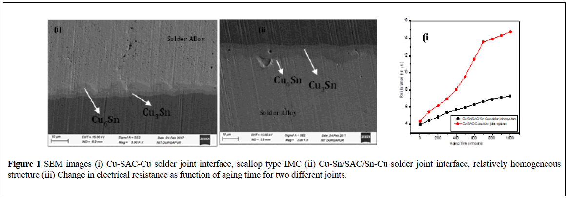
Two types of solder joints were prepared, one using SAC305 only (hereafter called Cu-SAC-Cu) and the other using SAC305 and tin interlayer (thereafter called Cu-Sn/SAC/Sn-Cu) while Cu plates were used as substrate in both the cases. For making Cu-Sn/SAC/Sn-Cu joints, thin films of tin were introduced between the SAC305 paste and each Cu substrate following identical method. These assemblies (Figure 1) were then placed in a pre-heated Infra-Red reflow oven at 230°C allowed it for bonding for 20 minutes. Further, the changes of electrical properties on the thermally exposed samples were evaluated.
Results and Discussion
Results suggest that use of multi-layered thin film of Sn could be a potential candidate in order to address different reliability issues related to the lead free solders at current time. Transient liquid phase soldering (TLPS) needs to be introduced in order to get the controlled growth of intermetallics at the interface and improve the functional and mechanical properties. TLPS along with the multilayered structured essentially can thus produce the solder joint at relatively low temperatures [5].
The importance of developing multi-layered thin film or nano scale solders is at it’s hype and application of such solders could resolve many issues in connection with the reliability and service life enhancement of the electronic gadgets. It is well known that the melting point of Sn/Pb solder is 183°C and the melting point of eutectic SAC alloy is approximately 217°C, about 34°C higher than that of the conventional Sn–Pb solders. While the processing/reflow temperature (RFT) of Sn/Pb solder is 210°C and that of eutectic SAC alloy is approximately 240°C respectively. So there is almost 30°C rise in processing temperature compared to SnPb alloy. This shall eventually enhance IMC formation at the (Cu-SAC-Cu) joint interface as the mass transport during processing becomes more abundant across the interface of the solder joint due to this huge difference between the MP and RFT. As a whole it is observed that total IMC density at the interface is higher compare to the conventional Sn/Pb soldered joints [6,7]. As a result the bond becomes brittle and weaker which further deteriorate during use and hence the overall life of the gadgets gets reduced. In order to address this issue, there is an urgent need of developing technologies for making solder joint at reasonably low temperature along with controlled IMC growth. This may be attained by using multilayered structured configurations as reported in this study.
Melting point depression in the nanostructured materials is a well-known phenomenon. Instead of using only the filler/solder alloy, introduction of Nano multilayers along with the solder paste shall be able to solder the copper substrates at relatively lower temperature. During processing, multilayered foils act as a local heat source, the energy released by selfpropagating exothermic reactions in multilayered foils can be harnessed to melt SAC solders in between the Cu substrates and help join them [8].
We have successfully demonstrated superior functional properties in the solder joints produced using (Cu-Sn/SAC305/Sn-Cu) multilayered structure. Solder joints prepared only using SAC305 solder paste appears to be inhomogeneous whereas the introduction of Multilayered thin film combination with SAC305 exhibits more homogeneous interface and . characterization of the as soldered/reflowed sample and sample after 1000hours of aging (at 150OC) reveals a higher electrical resistance for the only Cu-SAC305Cu soldered sample compare to Cu-Sn/SAC305/Sn- Cu solder joints. Microstructural changes and the electrical properties have been depicted in the (Figure 1).
The increment of the total IMC thickness in Cu-Sn/SAC/Sn-Cu solder joint is only 58.93% of its initial thickness after 1000hours of thermal aging at 150°C. Whereas the Cu-SAC-Cu joints, exhibits an increment of 73.30% under similar condition. Such difference in the IMC thickness is eventually reflected in the electrical resistance of the joint interface.
Conclusion
Solder joint interfacial microstructural growth kinetics could be controlled by using multilayered thin film of Sn in association with SAC305. Adapting the TLPS and thin multilayered structured configurations in soldering shall significantly help improve the service life of the gadgets and minimize the risk of premature failure.
REFERENCES
- Tu KN, Gausak AM, Li M. Physics and materials challenges for lead-free solders. J Appl Phys. 2003;93:13-35.
- Ramli MII, Mohd S, Mohd S. Effect of TiO2 additions on Sn-0.7Cu-0.05Ni lead free composite solder. Microelectronics Reliability. 2016;12188:9-10.
- QV Bui, ND Nam, JW Yoon, et al. Effect of gold on the corrosion behaviour of an electroless nickel/immersion gold surface finish. Journal of electronic materials. 2011;40:1937-42.
- Coyle RK, Sweatman BA. Thermal fatigue evaluation of Pb-free solder joints: Results, lessons learned, and future trends. J Miner Met.Mater Soc. 2015;67:2394-415.
- Chang DZ, Yu LG, Bin Y, et al. Nanoparticles of the Lead-free Solder Alloy Sn-3.0Ag-0.5Cu with Large Melting Temperature Depression. Journal of Electronic Materials. 2009;38:351.
- Shunfeng C, Chien MH, Michael P. A review of lead free solders for electronics applications. Microelectronics Reliability. 2016;75:77-95.
- Dong HJ, Li ZL, Song XG, et al. Grain morphology and mechanical strength of high-melting temperature intermetallic joints formed in asymmetrical Ni/An/Cu system using transient liquid phase soldering process.Journal of Alloys and Compounds. 2017;723:1026-1031.
- Tan AW, Tan F, Yusof. Influence of nanoparticle addition on the formation and growth of intermetallic compounds (IMCs) in Cu/SnAgCu/Cu solder joint during different thermal conditions. Science and Technology of Advanced Materials. 2015;16:033505.


