Formation of SiO2 and CrSi2 thin films on silicon surface and measurement of electrophysical parameters
Received: 04-May-2024, Manuscript No. puljpam-24-7101; Editor assigned: 05-May-2024, Pre QC No. puljpam-24-7101 (PQ); Accepted Date: Jun 17, 2024; Reviewed: 16-May-2024 QC No. puljpam-24-7101 (Q); Revised: 28-May-2024, Manuscript No. puljpam-24-7101 (R); Published: 31-Jul-2024, DOI: 10.37532/2752- 8081.24.8(4).01-03
Citation: Dovranov KT, Normuradov MT, Bekpulatov IR. Formation of SiO2 and CrSi2 thin films on silicon surface and measurement of electrophysical parameters. J Pure Appl Math. 2024; 8(4):01-03.
This open-access article is distributed under the terms of the Creative Commons Attribution Non-Commercial License (CC BY-NC) (http://creativecommons.org/licenses/by-nc/4.0/), which permits reuse, distribution and reproduction of the article, provided that the original work is properly cited and the reuse is restricted to noncommercial purposes. For commercial reuse, contact reprints@pulsus.com
Abstract
In this paper, we described the formation of SiO2 and CrSi2 thin films using a magnetron sputtering device. The surface morphology of the films was analyzed using ASM and SEM devices, and the elemental composition of the samples was determined using an energy-dispersive X-ray measurement device. Electrophysical quantities were determined using the HMS-5000 measuring device. According to the measurement results, it was confirmed that CrSi2 semiconductor nanofilms and SiO2 dielectric thin films were successfully grown by solid phase ion-plasma method. The charge carrier mobilities, bulk and sheet concentrations of the thin films are consistent with the values in the available literature. These layers are of practical importance in the use of sensors operating in the IR range. The nature of interactions through distance such as gravitational interaction, electromagnetic interaction, nuclear interaction, etc.
Key Words
Magnetron sputtering device; Mobilities; Gravitational interaction; Electromagnetic interaction; Thermal phenomena
Introduction
The metal silicides in thin films are of interest to materialsscientists. Although precision synthesis methods such as Molecular Beam Epitaxy (MBE) and Pulsed Laser Deposition (PLD) provide significant control over these systems, a gap remains between ideal and realized materials. We can consider that the solid-phase ion-plasma method of the magnetron dusting device is a method that eliminates these gaps. Because thin films have different structures and chemical compositions, it is often difficult to predict which properties will occur. High-resolution structural and chemical characterization methods are needed to validate growth models, relevant theoretical calculations, and materials design. The surface morphology of the thin films was analyzed using ASM and SEM devices, the energy dispersion spectrometer was used to analyze the elemental composition, and the electrophysical parameters were measured using the HMS-5000 measuring device provided by Ecopia CORP [1-4].
The synthesis of thin films formed in a magnetron sputtering installation is carried out using SiO2/Si and Si(111) substrates. Before forming the CrSi2 film, the SiO2/Si and Si(111) substrates were cleaned in two stages:
1.Cleaning the surface of Si(111) and SiO2/Si (d=60 mm)substrates was carried out by washing with deionizedwater at a temperature of 65°C -75°C using an ammonia-peroxide mixture and drying in a centrifuge;
2.Vacuum treatment (cleaning) of the surface of the siliconwafer was carried out using an argon plasma flow onto an advanced magnetron sputtering EPOS-PVD-DESK-PRO. The plasma current is created by a cold cathode ion source with a voltage of 2.4-3.6 kV and a current of up to 134 mA for (5, 6-8, 8) minutes. During treatment, a group of diapers (1÷3) pieces is placed in a rotating device.
CrSi2 films were formed on an EPOS-PVD-DESK-PRO magnetron sputtering installation at a pressure of 10–5 Pa and room temperature. The target purity of CrSi2 was 99.6%. The diameter and thickness of the target were 76 mm and 6 mm, respectively.
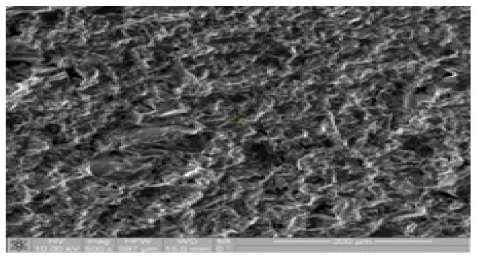
Before placing the target in a magnetron machine, its composition and structure were studied using a 3D Scanning Electron Microscope (SEM) Quanta 200 from the Dutch company FEI (Figure 1).
Figure 1: Results of studying the CrSi2 target using a Scanning Electron Microscope (SEM): surface image, and energy-dispersive X-ray spectrum, elemental composition of the sample
Elemental analysis of thin films of CrSi2 and SiO2 formed in an automated and modernized magnetron sputtering installation using energy-dispersive X-ray spectroscopy, surface morphology, structure and thickness of the films were studied using an SEM electron microscope (on a standard FEI Quanta 200 F installation) and high-energy electron diffraction DBED. To measure the electrical properties, an Ecopia HMS-5000 type device was used. All CrSi2 films were obtained at room temperature and were amorphous. The film was annealed at 750 K for 2 hours to obtain a polycrystalline structure.
The elemental composition of the samples was studied using energy-dispersive X-ray spectroscopy. Figure 2 shows an SEM image of an unheated CrSi2 film. The experiment was carried out on a Quanta 200 3D microscope. Table 1 shows the percentage of elements in CrSi2. As can be seen from the data presented, the sample contains the most chromium and silicon by mass and atomic percentage and very little oxygen (Figure 3).
TABLE 1 Energy dispersive spectrum quantitative results
| Element | Element | at. % |
|---|---|---|
| Si,K | 60,4 | 62,32 |
| Cr,K | 36,35 | 33,6 |
| O,K | 3,25 | 4,08 |
The table shows that oxygen is present in the smallest quantity. But a film produced by magnetron sputtering cannot contain S and O atoms. So these may be environmental atoms located on the surface of the film. A fragment of the surface was taken to study the distribution of elements in depth. The selected fragment represents the surface of the sample at an angle of 54 degrees. Thanks to this, a picture of the distribution of elements along the depth of the sample was obtained (Figure 3).
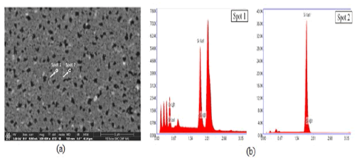
The SEM image (a) and energy-dispersive spectra (b) of the surface of CrSi2 films obtained by the solid-phase ion-plasma method are presented in figure 4. Films were obtained by magnetron sputtering onto the surface of a silicon substrate for 30 seconds. As can be seen from figure 4a, individual sections of the film with a size of 90 nm- 150 nm (black phases) are not coated with silicone.
Analysis of the energy-dispersive spectra of the CrSi2 surface (Figure 4b) shows that the concentration of Cr and Si at point 1 is about 33, 6 and 62, 32 at.%, which corresponds to the structure of CrSi2. Point 2 has a very low concentration of Cr atoms. It can be seen that a certain number of CrSi2 molecules are also present in uncoated Si sites. The Si(111) surface is completely covered with an amorphous CrSi2 film during sputtering within 60 s (∼400 Å). The SEM image and DBED pattern (inset) of a thin CrSi2 film formed on a silicon surface by magnetron sputtering for 120 s and then annealed at t=477Ë?C for 1 hour are shown in figure 5a.
Figure 5: a) SEM image and DBED pattern (inset) of a CrSi2 thin film formed by magnetron sputtering for 120s onto a silicon surface annealed at t = 477°C for 1 hour, b) SEM image of the cross section of a thin CrSi2 film formed on a silicon surface by magnetronsputtering for 120s and then annealed at 477°C for 1 hour
As can be seen from the figure, in this case a smooth and uniform polycrystalline CrSi2 film is formed. Figure 5b shows an SEM image of a cross section of a thin film of the CrSi2/Si(111) system. It can be seen that the film thickness is about 80 nm.
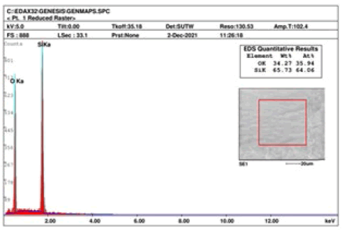
SEM of a thin film of Silicon Oxide (SiO2) obtained by a low-energy ion plasma method using a magnetron sputtering device, as well as the chemical composition and energy dispersive X-ray diffraction pattern of a SiO2 sample obtained after growing oxide layers 150 nm-250 nm thick at high temperature as a substrate prepared with using an energy dispersive device. Analyzes were performed under a Quanta 200-3D microscope (Scios FEI) (Figure 6). Results (O-wt.%-34.27,at%-35.94), (Si-wt.%-65.73, at%-64.06) elements were determined infractions.
In this section, the surface morphology and composition of SiO2 and CrSi2 films formed on the silicon surface were studied using a Quanta 200 3D Scanning Electron Microscope (SEM). CrSi2/Si(111) films were formed from a CrSi2 target using a modern EPOS-PVD-DESK-PRO sputtering magnetron. The composition of the resulting thin film of CrSi2 silicide and the chemical bonds formed in it has been studied.
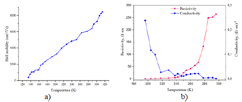
It should be noted that the Hall constant for the studied object changes with temperature within wide limits: when the temperature rises from 130 K to 300 K, it increases five times. As can be seen from Hall EMF measurements, the conductivity of the studied sample is p-type conductivity (Figure 7).
Figure 7a, 7b shows the temperature dependence of surface resistance, conductivity and specific resistance of SiO2 thin films formed by magnetron sputtering on the silicon surface using the HMS 5000 measuring device. According to the measurement results, with the increase in temperature, the conductivity decreased, the specific resistance and surface resistance increased sharply, which can be explained by the fact that the SiO2 film has dielectric properties.
Table 2 shows the electrophysical parameters of silicon oxide thin films produced by ion-plasma method with pure silicon and low-energy ions intended for use as a substrate.
TABLE 2 Results obtained on the HMS 5000 measuring device
| Parameters | Measurement value | Measurement result for Si substrate | Measurement results for SiO2 thin film |
|---|---|---|---|
| Input Current | 1 nA ÷ 20 mA | 5 mkm | 5 mkm |
| Bulk concentration (1/cm3) | 107 ÷1021 | 1,92·1014÷9,024·1015 | 1,24·1017÷ 7,16·1015 |
| Sheet concentration (1/cm2) | 107 ÷1017 | 11,437·1014 ÷ 1,443·1012 | 1,33·1015÷ 1,39·1014 |
| Mobility (cm2/Volt·sec) | 1÷107 | 984,06÷2478,3 | 11,143÷64,86 |
| Magnetic Flux Density(T) | 0.51Tesla (± 0.03T) | 0,53 Tesla (± 0.03T) | 0,54 Tesla (± 0.02T) |
| Temperature (K) | 80÷300 | 130÷300 | 190÷300 |
| Measurable Sample size | 5×5mm ~ 20×20mm size. Less than 2 mm thickness | 10×10mm | 10×10mm |
CrSi2 thin films grown by the solid-phase ion-plasma method were initially formed in an amorphous state on silicon and silicon oxide substrates. After thermal heating at 750 K for 1 hour, polycrystalline films were formed, as seen from the SEM and RHEED patterns. The elemental composition of the obtained films was studied, and their thickness was measured by SEM. Ne=2.584·1015 ± 0.5·1015 cm-3, nsh=1.44·1012 ± 0.5·1012 cm-2 and μH=31.87 ± 0.04 cm2·V-1·s-1 for amorphous SiO2 films at room temperature. It is equal to and slightly organ with decreasing temperature. This value is significantly smaller than the values reported for SiO2 amorphous films (Ne =4÷6·1020 cm-3)sputtered on a silicon wafer. This low mobility can be attributed tothe structural disorder inherent in amorphous dielectric compounds,which disperse charge carriers weakly. For CrSi2 films at roomtemperature Ne=1.584·1023 ± 0.3·1023 cm-3, nsh=1.44·1022 ± 0.4·1022cm-2 and μH=21.87 ± 0.04 cm2·V-1·s-1 is equal to. The mobility valuesrange from μH=3412.90 ± 0.8 cm2 V-1 s-1 to μH=3697.40 ± 0.12 cm2V-1s-1 for 80 nm thick films, respectively. These values remainsignificantly lower than those measured in the mass analogue.
Analysis of the research results shows that the CrSi2 thin film can be widely used as a semiconductor element to replace materials with p-type physical properties, as well as as active parts of modern micro- and nanoelectronic devices in the future.
References
- Schneider I, Bernoulli J, Conjectandi ARS. InLandmark Writings in Western Mathematics. Elsevier. 1713; 88-104.
- J. Worpitzky, Studien uber die Bernoullischen und Eulerschen Zahlen. J Reine Angew Math. 1883;94:203-32.
- Cesàro E. Sur une équation aux différences mêlées. Nouvelles annales de mathématiques. J des candidats aux écoles polytechnique et normale. 1885;4:36-40.
- D'Ocagne M. Sur les nombres de Bernoulli. Bulletin de la Société Mathématique de France. 1889;17:107-9.


